

Semiconductor_Manufacturing_Introduction README

The project's README from github.com/chenwei810/Semiconductor_Manufacturing_Introduction. As one markdown file: README.md.

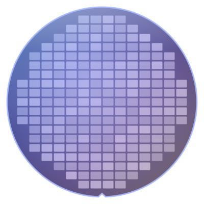
A silicon wafer covered with dies

半導體製造概論
Introduction to Semiconductor Manufacturing

繁體中文 | English | 日本語 | 한국어

License: CC BY-NC-SA 4.0 Chapters Languages Contributions welcome

An open, beginner-friendly book that follows one silicon wafer from sand, through the fab, test and packaging, until it becomes a chip. It skips heavy physics and focuses on process flow, terminology and know-how from the fab floor, with term boxes and know-how boxes in every chapter. No background in semiconductor physics is needed.


目錄 · Contents · 目次 · 목차

第 0 部 開始之前 · Part 0: Before You Start · 第 0 部 はじめる前に · 제0부 시작하기 전에

章 繁體中文 English 日本語 한국어
0 半導體製造全景 The Big Picture 半導体製造の全体像 반도체 제조의 전체 그림
1 晶圓廠如何運作 How a Fab Works ファブの仕組み 팹은 어떻게 돌아가는가

第 1 部 基礎 · Part 1: Fundamentals · 第 1 部 基礎 · 제1부 기초

章 繁體中文 English 日本語 한국어
2 從物理到電晶體 From Physics to Transistors 物理からトランジスタへ 물리에서 트랜지스터까지
3 從沙子到晶圓 From Sand to Wafer 砂からウェーハへ 모래에서 웨이퍼까지

第 2 部 製程模組 · Part 2: Process Modules · 第 2 部 プロセスモジュール · 제2부 공정 모듈

章 繁體中文 English 日本語 한국어
4 微影 Lithography リソグラフィ 리소그래피
5 薄膜 Thin Films 薄膜 박막
6 蝕刻 Etching エッチング 식각
7 離子佈植與熱處理 Ion Implantation and Thermal Processing イオン注入と熱処理 이온 주입과 열처리
8 CMP CMP CMP CMP
9 清洗與污染控制 Cleaning and Contamination Control 洗浄と汚染管理 세정과 오염 관리
10 金屬化 Metallization メタライゼーション 금속 배선

第 3 部 製程整合 · Part 3: Process Integration · 第 3 部 プロセスインテグレーション · 제3부 공정 통합

章 繁體中文 English 日本語 한국어
11 走一遍完整的 CMOS 流程 A Complete CMOS Process Flow CMOS プロセスフローを一通り CMOS 공정 흐름 한눈에 보기
12 先進電晶體結構 Advanced Transistor Structures 先端トランジスタ構造 첨단 트랜지스터 구조
13 記憶體製程 Memory Processes メモリのプロセス 메모리 공정
14 「幾奈米」是什麼意思 What Does "3 nm" Really Mean? 「何ナノ」とは何か '몇 나노'란 무엇인가

第 4 部 品質與良率 · Part 4: Quality and Yield · 第 4 部 品質と歩留まり · 제4부 품질과 수율

章 繁體中文 English 日本語 한국어
15 量測與檢測 Metrology and Inspection 計測と検査 계측과 검사
16 良率與故障分析 Yield and Failure Analysis 歩留まりと故障解析 수율과 불량 분석
17 製程控制 Process Control プロセス制御 공정 제어
18 異常處理與工程變更 Handling Abnormalities and Engineering Changes 異常処置と変更管理 이상 처리와 엔지니어링 변경

第 5 部 後段:測試與封裝 · Part 5: Back End — Test and Packaging · 第 5 部 後工程:テストとパッケージング · 제5부 후공정: 테스트와 패키징

章 繁體中文 English 日本語 한국어
19 晶圓測試 Wafer Test ウェーハテスト 웨이퍼 테스트
20 封裝 Packaging パッケージング 패키징
21 先進封裝 Advanced Packaging 先端パッケージング 첨단 패키징
22 最終測試與可靠度 Final Test and Reliability 最終テストと信頼性 최종 테스트와 신뢰성

第 6 部 走出晶圓廠 · Part 6: Beyond the Fab · 第 6 部 ファブの外へ · 제6부 팹 밖으로

章 繁體中文 English 日本語 한국어
23 工廠如何被系統管理 How Systems Run the Fab システムによるファブ運営 시스템이 팹을 운영하는 방법
24 製程如何影響韌體 How the Process Shapes Firmware プロセスとファームウェア 공정이 펌웨어에 미치는 영향

附錄 · Appendices · 付録 · 부록

繁體中文 English 日本語 한국어
A 術語總表 Glossary 用語集 용어집
B 現場行話 Fab Jargon 現場用語 현장 용어
C 延伸閱讀 Further Reading 参考文献 참고 자료

Reading paths

Path Chapters
🚀 Quick overview 0, 1, 11, 14
💻 Software and firmware engineers 0, 2, 11, 13, 14, 22, 23, 24
🏭 Joining the industry The whole book, especially 1, 11, 15–18 and Appendix B
📦 Packaging and test 0, 11, 19–22

Contributing

The original text is written in Traditional Chinese, and the other languages are translations of it. If this book helps you, please give it a ⭐ star so that more people can find it.


Disclaimer

This book is based on public information and general industry knowledge. It contains no confidential information, process parameters or internal procedures of any company, and it is not affiliated with any semiconductor company. Most numbers are orders of magnitude or approximate values; actual values vary by process, product and company.

License

The text and images are licensed under CC BY-NC-SA 4.0. You may share, adapt and translate them for non-commercial purposes, as long as you give credit and share your work under the same license.

Semiconductor_Manufacturing_Introduction (chenwei810/Semiconductor_Manufacturing_Introduction)

Searching Database…

这是什么?一本开放且对新手友好的书,追踪一片硅晶圆从沙子开始,经历晶圆厂、测试和封装,最终成为芯片的全过程。它侧重工艺流程、术语和晶圆厂实操知识,而非艰深的物理。
这是一本教科书,还是只是一个链接列表?它是一本结构化教科书,共 24 章,分为 7 个部分(基础知识、工艺模块、工艺集成、质量/良率、后道测试与封装、晶圆厂之外),另有 3 个附录:术语表、晶圆厂行话和延伸阅读。
我应该从哪里开始读?根据你的目标选择阅读路径:想快速了解全貌,读第 0、1、11、14 章;软件和固件工程师读第 0、2、11、13、14、22、23、24 章;如果打算进入这个行业,读整本书(尤其是第 1、11、15-18 章和附录 B);只关注封装和测试主题的话,读第 0、11、19-22 章。
读它需要半导体物理背景吗?不需要,这本书专为初学者设计,明确不要求任何半导体物理基础知识。
内容基于真实公司的工艺数据吗?不基于,本书只使用公开信息和通用行业知识,不含任何机密或公司内部数据,书中给出的大多数数字都是近似值或数量级数值。
我可以将本书用于商业用途或分享吗?不可以,文字和图片采用 CC BY-NC-SA 4.0 许可,因此仅可为非商业目的进行分享、改编和翻译,且需注明出处并对衍生作品适用相同许可。
这本书整体是如何组织的?全书分为 7 个部分,涵盖基础知识、各个工艺模块(光刻、薄膜、刻蚀、离子注入、CMP、清洗、金属化)、工艺集成、质量与良率、后道测试与封装,以及工艺如何与系统和固件衔接,最后以三个附录收尾。
这些阅读路径是为谁设计的?本书为只想快速了解概貌的读者、软件/固件工程师、即将进入半导体行业的人士以及封装/测试专家提供了量身定制的阅读路径。
Creator
chenwei810
Size
1.6 MB
Stars
1.2K
Updated
CommitOct 18
Age
8d
Commits · 90 Days